SPDM Tech

Chapter 3 · Coupled component models

Components as building blocks.

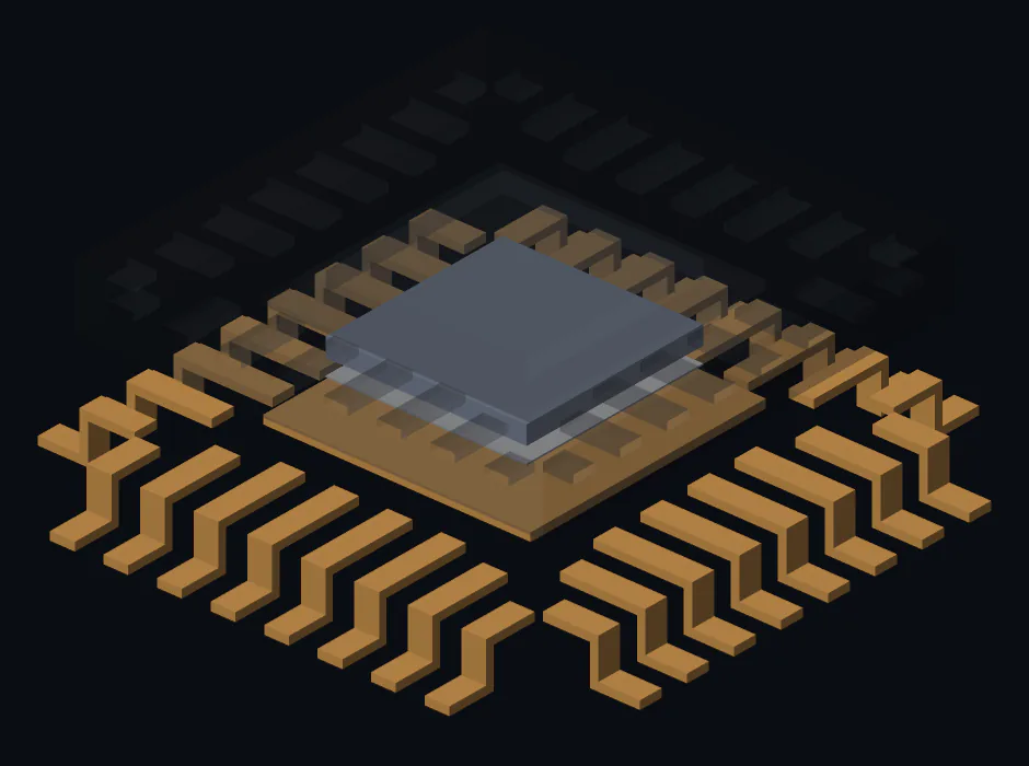
A reduced model for the chip package, one for the board, coupled at their pins. Junction, pins and board for any power profile, in milliseconds, with the accuracy of the full 3D models.

Talk to us
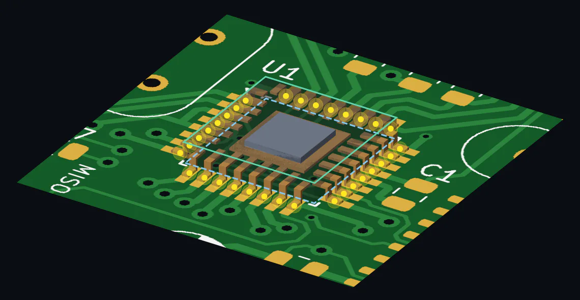
The TQFP-32 package on the circuit board, with its 32 lead ports marked
The microcontroller U1 on the board: 32 leads, the air gap under the body and the body surface are the 34 ports where the two models meet.
  • 424 584 → 357Unknowns: package and board in full 3D, and coupled as reduced models
  • 105.0 K/WFrom junction to air on this board. Similar devices list 63–69 K/W on a standard test board
  • 68 %Of the heat leaves through the 32 leads, 26 % through the air gap
  • 0.054 KLargest difference to the full models, anywhere in package and board, at any time

The result · 1 W in the die, steady state

From the die to the air, every path accounted for.

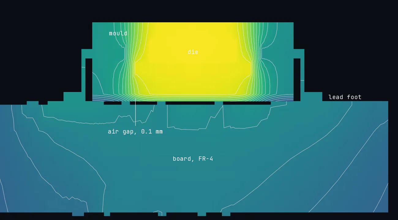
Section through the package and the board with isotherms: the die is hottest, the heat spreads through the leads and the air gap into the board
Section through a lead row: die, mould, lead feet, the 0.1 mm air gap and the board, with isotherms every 5 K.
Junction
+105.0 K
Pins
+34.4 … +53.9 K
Board under U1
+48.6 K

Where the watt goes

  • Leads → board → air683 mW
  • Air gap → board → air263 mW
  • Body surface → air55 mW

Temperatures are rises above ambient air. The pins differ by almost 20 K: the board, not the package, decides which pins run hot.

Try it

How much power can U1 take?

Set the ambient temperature, your junction limit and a power profile. The coupled reduced model answers right here, in your browser.

Junction Hottest pin Your limit Full models, 424 584 unknowns

Junction, peak
Margin
Allowed power
Computed in

How it works

Four steps, each one a script you can rerun.

  1. 1 · Component

    The package in 3D

    Die, die attach, copper die pad, 32 gull-wing leads and mould: 89 695 unknowns, calibrated to θJC = 20 K/W.

  2. 2 · Ports

    34 thermal ports

    Each lead foot on its pad, the air gap under the body and the body surface: where package and board exchange heat.

  3. 3 · Reduce and couple

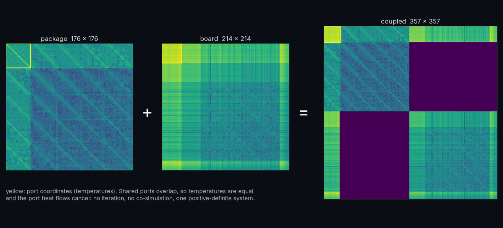
    176 + 214 → 357

    Each part reduced on its own, its port temperatures kept. Added at the ports: no iteration, no co-simulation.

  4. 4 · Check

    Against the full models

    Package and board in full 3D, coupled exactly: steady state, heat-up and pulses, node by node.

Document → data → model

Every input has an origin.

U1 is assumed to be an ATmega328P-AU; its own datasheet was not available and was not used. So every value in the package model is marked: taken from a document, from a standard, assumed or calibrated.

  1. source Board Gerber files Arduino Nano IO Shield-F_Cu.gbr (KiCad 8)
    • 32 pads · 0.8 mm pitch
    • no exposed pad
    TQFP-32, 7 × 7 mm, 32 lead ports

    Counted and measured from the pad flashes (32 pads, pitch 0.800 mm)

  2. source Manufacturer thermal data, 32-pin TQFP (other devices) Microchip online documentation for other AVR devices in 32-pin TQFP: 'Thermal Resistance Data' and 'Power Considerations'[1][2][3][4]
    • θJC 14.3–23.1 K/W → 20 K/W
    • θJA 63–69 K/W, check only
    calibration target, θJC = 20 K/W

    Not the ATmega328P itself: values of other devices in the same package

  3. standard Outline standard, TQFP JEDEC MS-026 (thin quad flat package), 7 x 7 mm, 0.8 mm pitch
    • 7 × 7 × 1.0 mm body
    • lead 0.37 × 0.127 mm
    outer geometry

    Consistent with the footprint (foot centred on the pad); the standard drawing was not retrieved

  4. assumed Typical construction engineering knowledge of TQFP construction
    • die 3 × 3 mm · pad 4 × 4 mm
    • die attach 25 µm
    inner geometry

    Not the real ATmega328P die and lead frame

  5. assumed Typical material data engineering knowledge of typical values
    • k: Si 148 · Cu 260
    • attach 2 · air 0.026 W/mK
    materials

    Typical values, no datasheet

  6. calibrated Own calculation θJC (top) of the package model: case top at 0 °C, 1 W on the die, other faces adiabatic
    • θJC = 20.0 K/W reached
    mould compound, k = 0.78 W/mK

    K = 0.78 W/(m K) lies in the typical range of mould compounds (0.6-1.0)

source
Taken from a document or file; checked where possible
standard
Standard outline values from engineering knowledge; the standard document itself was not retrieved
assumed
Typical values chosen by the engineer (Claude); to be replaced by measured or vendor data
calibrated
Fitted so that the model reproduces a source value

Method sources for the port concept, no numbers taken: JEDEC JESD15-4 DELPHI compact thermal models; JEDEC JEP181 / ECXML exchange format; Siemens Simcenter Flotherm BCI-ROM (FMU, VHDL-AMS).
The evidence

Every number comes with its check.

Coupling only helps if every block is right on its own and the assembly gives the same answer as the full models together.

Decision dossierTQFP-32 on the Nano IO Shield
  • Package model against CalculiXK and C identical to 3·10⁻⁸
  • θJC calibrated20.0 K/W → mould 0.78 W/mK
  • Steady state, coupled10⁻⁸ K against the full models
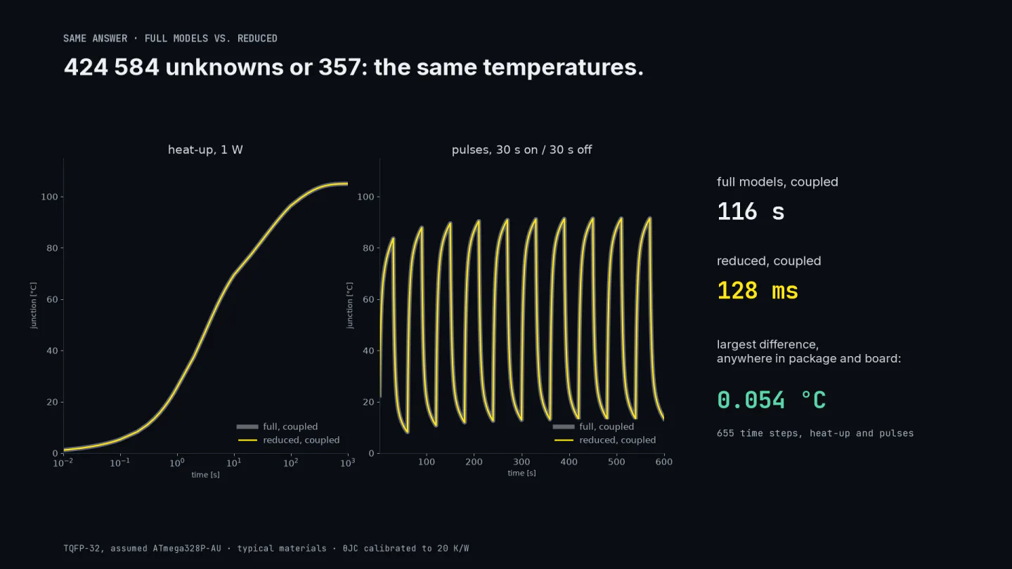
  • Heat-up and pulses≤ 0.054 K whole field, junction ≤ 0.002 K
  • Coupled system357 unknowns, positive definite
  • 655 time steps, heat-up and pulsesfull models 116 s, reduced 128 ms

Beyond this board

Build once, reuse on every board.

A library of components

One reduced model per package.

Built and checked once, then placed on any board: the coupling happens at the ports, in milliseconds.

  • Shown here: TQFP-32 on the Nano IO Shield
  • Every pin, not a two-resistor network
  • Swap a component without remeshing the board

Whole assemblies

More blocks, the same principle.

Further components, heat sinks, the housing: each one a block with its ports, the assembly stays small and exact.

  • Several chips on one board
  • Board in its housing
  • Derating for the real mission profile

Shared without the drawings

A model that does not reveal the design.

A reduced model passes on the thermal behaviour, not the geometry inside: a way for suppliers and customers to work with the same numbers.

  • Component makers to board designers
  • Board makers to system integrators
  • Into system simulation and digital twins

Shown with results on this page: one package coupled to one board. Several components, heat sinks and housings follow the same steps and are not shown here yet.

The whole story

Components as building blocks, in 85 seconds.

Assumptions: TQFP-32 7x7x1.0 mm, 0.8 mm pitch (assumed ATmega328P-AU) with typical materials; the mould conductivity is calibrated so that θJC = 20 K/W (where each input comes from: see above). Leads ideally soldered to their pads, a 0.1 mm air gap under the body, convection h = 12 W/m²K on the body surface; the board as on the PCB thermal page. The model is linear: temperature rises scale with power and are added to the ambient temperature, so the calculator's absolute temperatures assume constant material values and convection. 1 W is a reference load, well above what this microcontroller dissipates in normal use. The calculator uses 1 s time steps like the reference runs. Times measured on the same machine; the full models coupled exactly through their port heat flows.

Pilot partners wanted

Have a component that runs hot? Let's put a number on it.

SPDM Tech is in its build-up phase. As one of the first pilot partners, you bring one real question, from a circuit board, a drawing or a simulation process, and get a checked answer.

Become a pilot partner